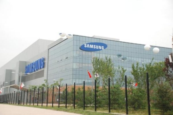

Samsung 2 nanometers no longer emphasize supercharger, but hopes that prices will become an alternative option
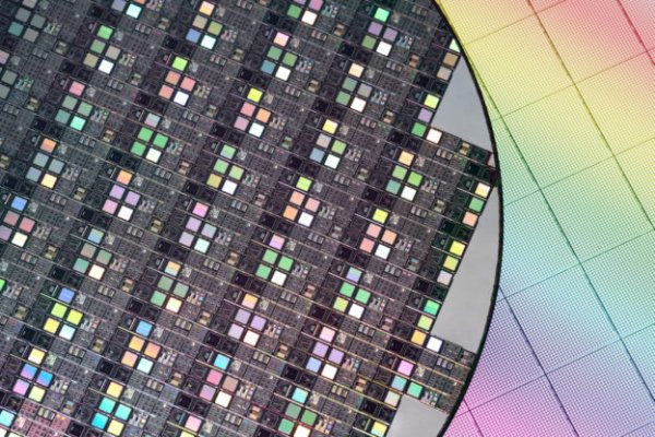
According to wccftech's report, South Korea's Samsung is gradually improving its 2-nanometer GAA stage process with the goal of improving yields and reducing costs, in order to become a strong replacement for NTIE solutions. Although TEK currently has no real rival in 2nm technology and is expected to start mass production of 2nm technology in 2025. However, Samsung is working hard to narrow the gap with TEK through the optimization of its own 2-nanometer GAA technology.
The Samsung yield challenge is a road of turbulence. Because Samsung is adopting a more cautious strategy in improving the yield of 2 nanometers of GAA. However, market news pointed out that Samsung is gradually improving its microfilm technology to improve yields. Moreover, Samsung has decided to delay the introduction time of its 1.4-nanometer process and turn its focus entirely on optimizing the 2-nanometer GAA process, which is considered to be the right decision.
Daily report on North Korea, Samsung plans to launch a variety of versions of the 2nm GAA process. Samsung internally predicts that market demand for 2nm GAA crystals will continue for at least three years, and may even last for four years. During this period, Samsung focused on solving heat dissipation problems and stabilizing performance. In this regard, a strategy has been launched, with the goal of focusing on the 2-nanometer GAA process and increasing its yield to 60% to 70%. Although these numbers are lower than NT$' yield, the current results are better than the company's previous expectations, so they will continue to proceed.
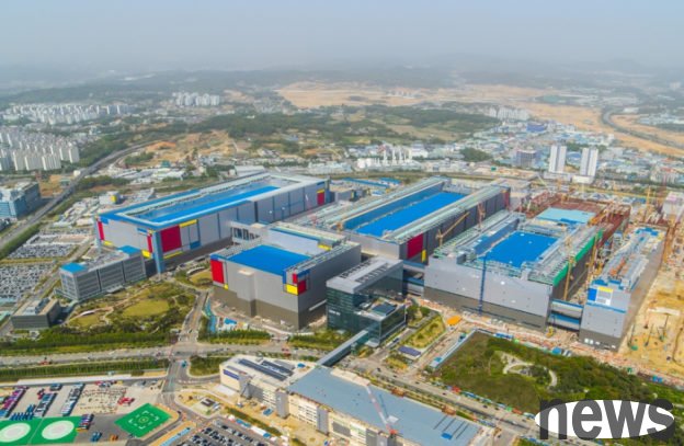
Samsung's strategy includes the 2-nanometer GAA process starting in the second half of the year, and Samsung has also established production lines in Pingze crystal plants and other locations. In addition, Samsung plans to launch a modified version of the 2nm GAA technology, where the basic design of the second-generation process may have been completed. As for the third generation process, the third generation process is named "SF2P+", Samsung's goal has been implemented within two years, but it has not yet been confirmed whether it will invest in the above-mentioned crystal factory or whether it will build new facilities.
Considering Samsung's past performance, it may not be subject to future orders. Samsung must attract customers with a 2-nanometer GAA crystal discount and build trust with customers. Although Samsung is still unable to compare and discuss with NTD, it is likely to improve its competitiveness in several years. Therefore, Samsung is working hard to overcome technical challenges and gradually improves 2-nanometer competition with practical strategies to become a TEK alternative.